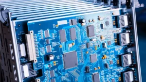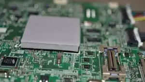
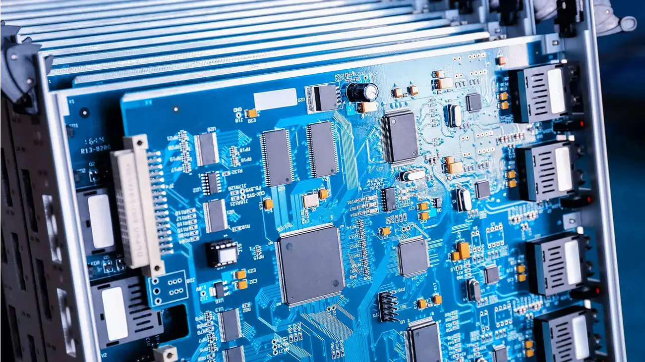
When designing high-density electronic control units (ECUs) for the automotive and industrial automation sectors, a frequent challenge is the forced coexistence of high-frequency microprocessors and bulky heatsinks. This tight geometric proximity often triggers destructive cavity resonances and rapid overheating of printed circuit boards.
To overcome these physical limitations without adding mechanical bulk to the PCB, materials engineering is decisively moving toward Multifunctional Solutions.
Instead of designing a complex multi-layer hardware package consisting of a metal shield, a standard thermal pad, and a separate electromagnetic absorber sheet, modern layout design adopts a single Hybrid Thermo-Magnetic Gap Filler. This integrated material delivers three immediate engineering and financial advantages:
- Reduction of Thermal Impedance: Eliminating multiple interfaces optimizes net heat transfer from the critical component to the cooling element, lowering overall operating temperatures.
- At-the-Source EMI Suppression: Special magnetic absorbing fillers integrated directly into the polymer matrix attenuate high-frequency noise and surface currents right where they are generated.
- Bill of Materials (BoM) Simplification: Using a single part number instead of three slashes inventory costs, accelerates assembly line cycle times, and eliminates risks tied to the stack-up of mechanical tolerances during production.
The technical team at Euro Technologies is fully available to analyze your printed circuit board layouts and configure the optimal hybrid compound to streamline and protect your design.
Contact our team for a personalized technical consultation on your layout.